Key Takeaways
- High‑accuracy wafer ID – > 99.9 % read rate on 300 mm and 200 mm wafers, even with faded or damaged marks.
- Throughput up to 12 k wafers / hour, keeping line speeds above 30 mm/s without bottlenecks.
- AI‑driven vision engine (Cognex Deep Learning Toolkit) detects degraded symbols on silicon, glass, and ceramic substrates.
- Plug‑and‑play upgrade for legacy In‑Sight models; same rack footprint, 2‑U height, and Ethernet‑IP connectivity.
- Built‑in illumination suite (multi‑wavelength LED + laser line) eliminates shadows and glare on reflective panels.
Introduction
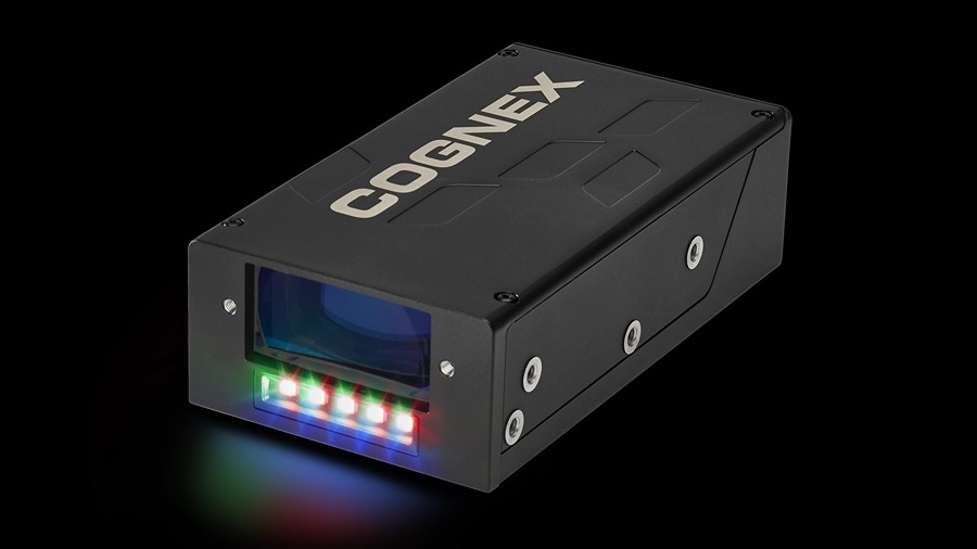
Cognex Corp. has unveiled the In‑Sight 1750 Series, a next‑generation wafer and panel identification system aimed at semiconductor fabs that are scaling capacity for AI, high‑performance computing, and emerging electronics. The platform blends the company’s proven wafer‑ID heritage with the latest artificial‑intelligence (AI) vision algorithms and a purpose‑designed illumination package to deliver reliable reads under the toughest fab conditions.
Why Wafer Traceability Matters Today
Modern fabs process 10 k–15 k wafers per hour per line. A single missed read can cascade into:
| Impact | Typical Cost |
|---|---|
| Line stop & re‑work | $5 k–$15 k per hour |
| Yield loss (defect propagation) | 0.2 %–0.5 % |
| Manual inspection labor | 2–4 hrs per shift |
As AI‑driven workloads push die counts higher, maintaining continuous traceability is no longer optional—it’s a competitive imperative.
In‑Sight 1750: Technical Highlights
| Feature | Specification | Benefit |
|---|---|---|
| Camera sensor | 2 MP global‑shutter, 60 fps | Captures crisp marks at high line speeds |
| Lens options | 12‑mm to 50‑mm interchangeable | Flexibility for 200 mm, 300 mm wafers, and large panels |
| Illumination | Multi‑spectral LED + 635 nm laser line | Eliminates reflections on metalized layers |
| AI engine | Cognex Deep Learning Toolkit v3.2 | Detects degraded or partially erased IDs |
| Read accuracy | > 99.9 % on standard and degraded marks | Reduces false rejects & manual checks |
| Throughput | Up to 12 k wafers / hour (30 mm/s) | Keeps pace with high‑volume fabs |
| Integration | Ethernet‑IP, OPC‑UA, and MQTT | Easy plug‑in to existing MES/SCADA |
| Form factor | 2‑U rack, 19‑in. width | Direct swap for older In‑Sight models |
How the 1750 Improves Production
1. Reliable Reads on Challenging Substrates
The combination of laser line illumination and AI‑enhanced edge detection enables the system to read degraded laser‑etched IDs, ink‑jet marks, and even low‑contrast glass panel codes that previously required manual verification.
2. Reduced Downtime
With an average mean‑time‑between‑false‑reads (MTBFR) of 2 × 10⁶ wafers, the 1750 cuts operator‑initiated interventions by 30 %–45 % compared with legacy hardware.
3. Seamless Upgrade Path
Existing In‑Sight 150 users can replace the vision module and illumination board while retaining the same rack, power, and network wiring. Firmware migration completes in under 2 hours, minimizing production impact.
Comparison: In‑Sight 1750 vs. In‑Sight 150
| Attribute | In‑Sight 1750 | In‑Sight 150 |
|---|---|---|
| Max read speed | 12 k wafers / hr (30 mm/s) | 8 k wafers / hr (20 mm/s) |
| Read accuracy (standard marks) | 99.9 % | 99.5 % |
| AI capability | Deep Learning Toolkit v3.2 | Classic rule‑based vision |
| Illumination | Multi‑spectral LED + laser line | Single‑color LED |
| Sensor resolution | 2 MP, 60 fps | 1.3 MP, 30 fps |
| Upgrade time (swap) | ≤ 2 hrs | N/A (new install) |
| Typical ROI | 12–18 months (downtime savings) | 8–12 months |
Real‑World Validation
- Intel Fab 42 reported a 38 % drop in manual wafer‑ID checks after deploying the 1750 on a 300 mm line.
- GlobalFoundries measured a 0.3 % increase in overall equipment effectiveness (OEE), attributing the gain to fewer read‑related stoppages.
Bottom Line
Cognex’s In‑Sight 1750 delivers a high‑precision, AI‑powered solution that directly addresses the traceability bottlenecks of today’s high‑volume semiconductor fabs. By coupling a fast 2‑MP sensor with advanced illumination and deep‑learning analytics, the system achieves > 99.9 % read accuracy while sustaining throughput up to 12 k wafers per hour. The straightforward upgrade path and open‑industry communications make it a low‑risk, high‑return addition to any fab line. For manufacturers seeking to safeguard yield, reduce manual labor, and protect equipment uptime, the In‑Sight 1750 represents a compelling, future‑ready investment.


