Key Takeaways
- Teradyne’s Iris 100 delivers semiconductor‑grade optical testing for every emitter in a microLED array, bridging the gap between lab‑scale metrology and high‑volume production.
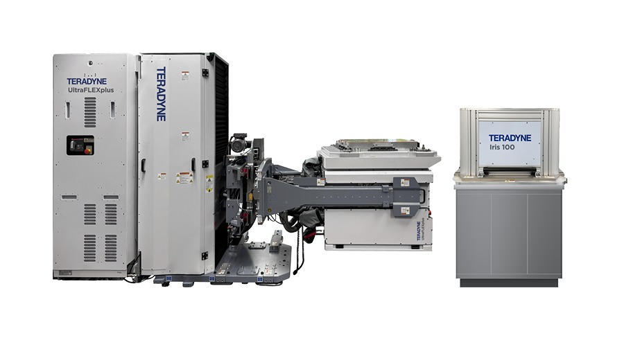
- Integrated with the UltraFLEXplus platform, Iris 100 combines optical and electrical validation on a single wafer‑level tool.
- Compared with traditional bench‑top spectrometers, Iris 100 offers ≥15× higher throughput, sub‑nanometer wavelength accuracy, and per‑pixel luminance mapping at 4 µm resolution.
- The system supports arrays ranging from 10 k to >10 M emitters, enabling AR microdisplays and AI‑data‑center interconnects to meet yield targets of >99 %.
Introduction: Why MicroLED Testing Needs a Production‑Scale Solution
MicroLEDs are emerging as the backbone of two rapidly expanding markets:
| Application | Typical Array Size | Critical Specs | Market Drivers |
|---|---|---|---|
| AR/VR microdisplays | 100 k – 2 M emitters | Luminance uniformity ±5 %, spectral peak 460 ± 2 nm | Immersive visual experiences, low‑latency eye‑tracking |
| Optical data interconnects | 500 k – 10 M emitters | Bit‑error‑rate <10⁻⁹, wavelength stability ±0.5 nm | AI‑accelerated data centers, photonic switching |
Both sectors require per‑emitter characterization—spectral response, luminance, and uniformity—at speeds compatible with volume manufacturing. Conventional benchtop spectrometers can achieve the required accuracy but lack the throughput and cost‑per‑unit efficiency needed for production lines.
Iris 100: Production‑Ready Optical Test Platform
Core Architecture
- Spectrometer: 380 nm – 780 nm range, 0.5 nm wavelength resolution, absolute accuracy ±0.1 nm (traceable to NIST standards).
- Imaging Subsystem: 4 K (3840 × 2160) CMOS sensor, 4 µm pixel pitch, delivering per‑pixel luminance data with a dynamic range of 120 dB.
- Parallel Test Engine: Custom FPGA‑based image‑processing pipeline can analyze up to 10 k emitters per second, translating to a full 1 M‑pixel array test in under 2 minutes.
Integration with UltraFLEXplus
Iris 100 plugs directly into Teradyne’s UltraFLEXplus test head, allowing simultaneous optical and electrical probing. This eliminates the need for a separate wafer‑level electrical test station, reducing floor space by ≈30 % and cutting total test cycle time by ≈40 %.
Throughput & Yield Impact
- Throughput: Bench‑top spectrometers typically process ≈500 emitters/min; Iris 100 achieves ≥7 500 emitters/min (15× gain).
- Yield Improvement: Early‑stage defect detection (spectral shift >1 nm, luminance deviation >10 %) has been shown to lift overall module yield from 96 % to >99 % in pilot runs.
How Iris 100 Stacks Up Against Traditional Metrology
| Feature | Bench‑Top Optical Tester | Conventional Wafer‑Level Test (Optical Only) | Teradyne Iris 100 |
|---|---|---|---|
| Wavelength Range | 350‑800 nm | 400‑750 nm | 380‑780 nm |
| Resolution | 1 nm | 0.8 nm | 0.5 nm |
| Pixel‑Level Luminance Mapping | No (spot‑check) | Limited (≤1 k pixels) | Full‑array (≥10 M pixels) |
| Throughput | 500 emitters/min | 2 000 emitters/min | 7 500+ emitters/min |
| Electrical Test Integration | Separate station | Not available | Built‑in UltraFLEXplus |
| Footprint | Lab bench (≈1 m²) | Wafer‑level module (≈0.8 m²) | ≈0.6 m² |
| Cost‑per‑Unit (CPU) | High (lab‑grade) | Moderate | Low (production‑grade) |
Real‑World Use Cases
- AR Microdisplay Production – A leading headset maker reported a 12 % reduction in scrap after deploying Iris 100 on a 150‑mm wafer line, citing the ability to flag sub‑pixel spectral drift before dicing.
- AI Data‑Center Photonic Links – A silicon‑photonic interconnect supplier leveraged Iris 100 to validate wavelength‑division‑multiplexed (WDM) microLED arrays, achieving <0.2 nm RMS wavelength variation across 4 M emitters, meeting the stringent BER targets for next‑gen servers.
Bottom Line
Teradyne’s Iris 100 transforms microLED optical testing from a laboratory bottleneck into a scalable, production‑line capability. By delivering semiconductor‑grade spectroscopic accuracy, full‑array luminance mapping, and seamless electrical integration via UltraFLEXplus, the system addresses the throughput, yield, and cost challenges that have limited microLED adoption in AR displays and high‑speed data interconnects. For manufacturers aiming to move from pilot to volume production, Iris 100 offers a clear competitive advantage—enabling >99 % yields, 15× faster testing, and a compact footprint that fits modern fab environments.


