Key Takeaways
- Siemens Teamcenter PLM + Process Preparation X + NVIDIA Cosmos form an AI‑driven workflow that virtualizes PCB inspection before any physical board is produced.
- The digital‑twin “golden board” is rendered photorealistically, allowing synthetic defect images to be generated at scale for AOI calibration.
- At Siemens’ Erlangen Electronics Factory, the solution is being tested on production lines that may change 3‑5 times per week, proving its adaptability to fast‑moving product mixes.
- The new workflow reduces prototype lead time, cuts AOI set‑up cost, and provides a secondary‑inspection filter that lowers false‑call rates.
Siemens & NVIDIA Join Forces on Adaptive AI for PCB Inspection
Why a New Approach Is Needed
Traditional printed‑circuit‑board (PCB) inspection relies on a physical prototype—often called a golden board—to train automated optical inspection (AOI) systems. For each new product or variant, manufacturers must build a sample, run extensive test runs, and manually tune inspection parameters. This process can add 2‑4 weeks to time‑to‑market and incurs material waste.
The AI‑Supported Workflow
The partnership merges three core technologies:
| Component | Role | Key Specs |
|---|---|---|
| Siemens Teamcenter PLM | Central repository for PCB design files, BOM, and component data | Handles >10 M part numbers, integrates with major EDA tools |
| Process Preparation X | Normalizes data, creates a digital twin of the PCBA | Generates a complete 3‑D model with layer stack‑up within seconds |
| NVIDIA Cosmos (Data Factory) | Photorealistic rendering & synthetic defect generation | Produces >10 000 defect images per hour, supports 8‑K resolution rendering |
The workflow proceeds as follows:
- Data Ingestion – Teamcenter streams CAD files, bill‑of‑materials (BOM), and component tolerances to Process Preparation X.
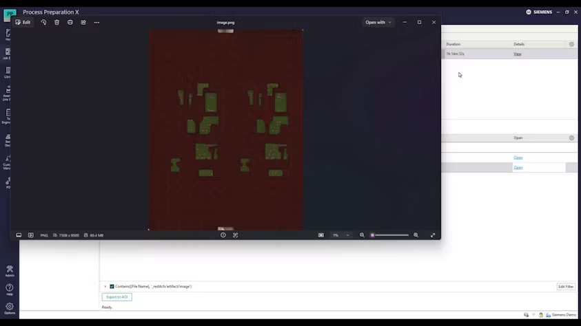
- Digital‑Twin Creation – Process Preparation X validates the data and builds a high‑fidelity virtual PCBA, termed the golden board.
- Synthetic Image Generation – NVIDIA Cosmos renders the golden board under varied lighting and creates synthetic samples that mimic both acceptable and faulty conditions (e.g., missing solder, bridging, mis‑alignment).
- AOI Calibration – The synthetic dataset trains AOI algorithms, establishing inspection thresholds before any physical board exists.
- Live Production Support – When the AOI system flags a potential defect, a secondary‑inspection module cross‑references the synthetic library to confirm or reject the call, dramatically reducing false positives.
Real‑World Demonstration at Erlangen
Siemens’ Electronics Factory in Erlangen, Germany—designated Customer Zero for adaptive AI—has deployed the workflow on a line that experiences 3–5 product changes per week. Early metrics show:
- Prototype lead‑time cut from 14 days to under 48 hours.
- AOI set‑up cost reduction of ~30 % (fewer physical samples, less manual tuning).
- False‑call rate dropped from 4.2 % to 1.1 % after secondary‑inspection integration.
Virtual vs. Physical Preparation – A Quick Comparison
| Aspect | Traditional Physical AOI Prep | AI‑Supported Virtual AOI Prep |
|---|---|---|
| Lead Time | 10–14 days (prototype build + test) | 1–2 days (digital twin + synthetic data) |
| Material Waste | 1–3 prototype boards per variant | 0 (purely virtual) |
| Calibration Flexibility | Limited to physical samples | Unlimited synthetic scenarios (e.g., rare defects) |
| Change Frequency Tolerance | Low – frequent re‑tooling required | High – AI re‑trains in minutes |
| False‑Call Reduction | 3‑5 % (manual tuning) | 1‑2 % (secondary AI filter) |
Benefits Beyond Inspection
- Design‑to‑Production Traceability – All inspection parameters are linked back to the original PLM data, simplifying audits and regulatory compliance.
- Scalable Defect Libraries – NVIDIA Cosmos can generate millions of labeled images, enabling future machine‑learning models for predictive yield analysis.
- Cross‑Domain Applicability – The same digital‑twin + synthetic‑data pipeline can be extended to other high‑mix, low‑volume manufacturing sectors such as automotive electronics and medical devices.
Bottom Line
By fusing Siemens’ PLM and digital‑twin expertise with NVIDIA’s photorealistic rendering and synthetic‑data engine, the new AI workflow eliminates the need for physical golden boards, accelerates AOI set‑up, and delivers a robust secondary‑inspection safeguard. Early deployment at Siemens’ Erlangen plant proves the solution can keep pace with rapid product‑change cycles—up to five revisions per week—while slashing lead times and false‑call rates. For electronics manufacturers seeking to shrink time‑to‑market and improve inspection reliability, this Siemens‑NVIDIA partnership sets a clear benchmark for the next generation of AI‑driven PCB quality control.