Key Takeaways
- M31 Technology ve Ambiq, TSMC’nin 12 nm N12e düğümü için ultra-düşük-güç (ULL) Foundation IP yığını ortak geliştirdi.
- Teklif, sızıntıyı yaklaşık %50 azaltan ve yakın-eşik modda performansı 500 MHz’in üzerinde tutan yüksek-yoğunluklu bir SPSRAM bellek derleyicisi ve özel bir standard-cell kütüphanesini bir araya getiriyor.
- AIoT, giyilebilir cihazlar ve her zaman-açık kenar cihazları için tasarlanmış bu IP, taslak-çıktı takvimlerini hızlandırıyor ve silikon alanını azaltıyor.
Introduction
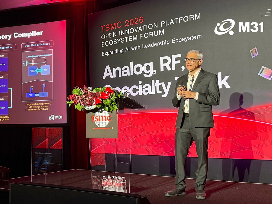
TSMC 2026 Kuzey Amerika Açık İnovasyon Platformu (OIP) Ekosistem Forumu’nda, M31 Technology ve Ambiq, TSMC’nin N12e sürecine dayanan tasarım-hazır bir Foundation IP çözümünü tanıttı. Ortaklık, modern sistem-üzerinde-çip (SoC) tasarımlarının “her zaman-açık” kalması ve AI-tabanlı işlevsellik sunması gerektiği durumlarda güç-bütçesi ve çip-büyüklüğü kısıtlamalarını hedefliyor.
Core Components of the Foundation IP
SPSRAM Ultra-Low-Leakage Memory Compiler
- Process: TSMC N12e ULL (Ultra-Low-Leakage)
- Architecture: Çift-raylı, aynı fiziksel ayak izinde yüksek-performans (HP) ve ultra-düşük-güç (ULP) modlarını destekler.
- Speed: Yaklaşık 500 MHz çalışma, yakın-eşik çevre voltajında (≈ 0.5 V).
- Leakage: Çevre (VCCA) tutma sızıntısı, bit-hücre tutma sızıntısının 1.05–1.10 × içinde kalır.
- Features: Yerleşik yedeklilik, güç-kapama ve yerleşik kendini test (BIST).
Derleyicinin devre topolojisi ve yerleşim optimizasyonu, minimum alan ek yüküyle yüksek-yoğunluklu bir makro oluşturur ve katı güç kısıtlamalarını karşılar. Erken silikon çalışmaları, eski 28 nm SRAM bloklarına göre %10-15 PPA (performans-güç-alan) iyileştirmesi gösterdi.
N12e Ultra-Low-Leakage Standard-Cell Library
- Leakage Reduction: Geleneksel bir N12e kütüphanesine göre ~%50 daha düşük statik güç, tipik hücre aileleri (invertörler, NAND/NOR, flip-floplar) arasında doğrulandı.
- Design Collaboration: Ambiq’nin kademeli-stil güç-yönetim metodolojisi, M31’in transistör-seviyesi ve yerleşim iyileştirmeleriyle birleştirildi.
- Compatibility: Ambiq’nin Apollo™ mikrodenetleyici aileleri için tam uyumlu ve herhangi bir N12e-tabanlı SoC’ye entegrasyona hazır.
Kütüphane, tasarımcıların agresif “her zaman-açık” güç hedeflerini (tipik 1 MHz sensör hubı için standby <10 µW) karşılamasını sağlarken kenar AI çıkarımı için gereken işlem gücünden ödün vermez.
Performance Highlights
| Metric | SPSRAM Compiler | Standard-Cell Library | Typical Legacy N12e IP |
|---|---|---|---|
| Leakage Power | 1.05-1.10 × bit-cell retention | ~50 % reduction | Baseline |
| Max Frequency (ULP mode) | ~500 MHz @ 0.5 V | 300-350 MHz @ 0.6 V | 250-300 MHz |
| Area Efficiency | 0.85 × of comparable 28 nm SRAM | 0.9 × of standard N12e cells | 1.0 × |
| Power-per-Operation | 0.8 pJ/bit read/write | 0.4 pJ/logic toggle | 0.7 pJ/bit |
| Time-to-Market | 4-6 weeks IP integration | 3-5 weeks library qualification | 8-10 weeks |
Tablo, bellek ve mantık IP’sinin geleneksel N12e çözümlerine göre birleşik avantajını, özellikle güç-kısıtlı kenar iş yükleri için vurgular.
Market Implications for AIoT and Wearables
Yeni Foundation IP, bir sonraki nesil kenar cihazları için üç temel sorunu doğrudan çözüyor:
- Power-Budget Tightening – Bekleme akımları tek haneli mikro-amper seviyelerine indiğinde, %50 sızıntı kesintisi tipik giyilebilir cihazlar için 2 yılı aşan pil ömürleri sağlar.
- Silicon Real Estate – Yüksek-yoğunluklu SPSRAM, 28 nm bloklarla karşılaştırıldığında SRAM ayak izini %15’e kadar azaltarak çip alanını ek sensör ön-uçları veya AI hızlandırıcıları için serbest bırakır.
- Design Velocity – Ön-kalifiye IP blokları ve birleşik doğrulama akışı, taslak-çıktı döngülerini yaklaşık %30 kısaltır; bu, hızlı hareket eden tüketici pazarlarında kritik bir avantajdır.
Bottom Line
M31 Technology ve Ambiq’nin TSMC’nin N12e düğümü için ortak Foundation IP’si, ultra-düşük sızıntı, yüksek-hızlı bellek ve güç-optimize standard-cell’lerin çekici bir kombinasyonunu sunar. Statik gücü yarıya indirip yakın-eşik modda >500 MHz çalışma sağlanarak, çözüm AIoT ve giyilebilir tasarımcıların agresif güç-alan bütçelerini karşılamasını ve ürün lansmanını hızlandırmasını mümkün kılar. Her zaman-açık kenar uygulamaları için bu IP yığını, daha uzun pil ömrü, daha küçük silikon ve daha hızlı pazara çıkış anlamında somut bir adım temsil eder.